


 Designer’s Notebook: What Designers Need to Know About Manufacturing, Part 2
 The Pulse: Drilling Down on Documentation
 Connect the Dots: Designing for Reality: Prioritizing Manufacturability
Intel Unveils Industry-Leading Glass Substrates to Meet Demand for More Powerful Compute
September 18, 2023 | IntelEstimated reading time: 3 minutes
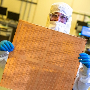
Intel announced one of the industry’s first glass substrates for next-generation advanced packaging, planned for the latter part of this decade. This breakthrough achievement will enable the continued scaling of transistors in a package and advance Moore’s Law to deliver data-centric applications.
“After a decade of research, Intel has achieved industry-leading glass substrates for advanced packaging. We look forward to delivering these cutting-edge technologies that will benefit our key players and foundry customers for decades to come,” said Babak Sabi, Intel senior vice president and general manager of Assembly and Test Development.
Compared to today’s organic substrates, glass offers distinctive properties such as ultra-low flatness and better thermal and mechanical stability, resulting in much higher interconnect density in a substrate. These benefits will allow chip architects to create high-density, high-performance chip packages for data-intensive workloads such as artificial intelligence (AI). Intel is on track to deliver complete glass substrate solutions to the market in the second half of this decade, allowing the industry to continue advancing Moore’s Law beyond 2030.
By the end of the decade, the semiconductor industry will likely reach its limits on being able to scale transistors on a silicon package using organic materials, which use more power and include limitations like shrinkage and warping. Scaling is crucial to the progress and evolution of the semiconductor industry, and glass substrates are a viable and essential next step for the next generation of semiconductors.
As the demand for more powerful computing increases and the semiconductor industry moves into the heterogeneous era that uses multiple “chiplets” in a package, improvements in signaling speed, power delivery, design rules and stability of package substrates will be essential. Glass substrates possess superior mechanical, physical and optical properties that allow for more transistors to be connected in a package, providing better scaling and enabling assembly of larger chiplet complexes (called “system-in-package”) compared to organic substrates in use today. Chip architects will have the ability to pack more tiles – also called chiplets – in a smaller footprint on one package, while achieving performance and density gains with greater flexibility and lower overall cost and power usage.
Glass substrates will initially be introduced into the market where they can be leveraged the most: applications and workloads requiring larger form factor packages (i.e., data centers, AI, graphics) and higher speed capabilities.
Glass substrates can tolerate higher temperatures, offer 50% less pattern distortion, and have ultra-low flatness for improved depth of focus for lithography, and have the dimensional stability needed for extremely tight layer-to-layer interconnect overlay. As a result of these distinctive properties, a 10x increase in interconnect density is possible on glass substrates. Further, improved mechanical properties of glass enable ultra-large form-factor packages with very high assembly yields.
Glass substrates’ tolerance to higher temperatures also offers chip architects flexibility on how to set the design rules for power delivery and signal routing because it gives them the ability to seamlessly integrate optical interconnects, as well as embed inductors and capacitors into the glass at higher temperature processing. This allows for better power delivery solutions while achieving high-speed signaling that is needed at much lower power. These many benefits bring the industry closer to being able to scale 1 trillion transistors on a package by 2030.
Intel has been researching and evaluating the reliability of glass substrates as a replacement for organic substrates for more than a decade. The company has a long history of enabling next-generation packaging, having led the industry in the transition from ceramic package to organic package in the 1990s, being the first to enable halogen and lead-free packages, and being the inventor of advanced embedded die packaging technologies, the industry’s first active 3D stacking technologies. As a result, Intel has been able to unlock an entire ecosystem around these technologies from equipment, chemical and materials suppliers to substrate manufacturers.
Building on the momentum of recent PowerVia and RibbonFET breakthroughs, these industry-leading glass substrates for advanced packaging demonstrate Intel’s forward focus and vision for the next era of compute beyond the Intel 18A process node. Intel is on the path to delivering 1 trillion transistors on a package by 2030 and its ongoing innovation in advanced packaging including glass substrates will help achieve this goal.
Share on:


Suggested Items
Real Time with... IPC APEX EXPO 2024: all4-PCB, A Premier Solution Provider for the PCB Industry
04/22/2024 | Real Time with...IPC APEX EXPOIn the PCB industry, all4-PCB, is a top-tier equipment supplier and process solution provider. Ralph Jacobo highlights the active market and the demand for high-quality equipment, discusses their existing customers, investment in advanced substrates, and smaller board shops.
PCB007 Magazine April 2024 — The Growing Industry Issue
04/15/2024 | I-Connect007 Editorial TeamAfter more than two decades of steady decline in the U.S., the PCB industry is finally growing in the West thanks to the CHIPS and Science Act, DoD funding, and hopefully, the passing of HR 3249, the Printed Circuit Board and Substrates Act. The U.S. is now in a race to regain what was lost and then some. But what does “growing” look like for the organizations that have received DoD funding, and for the rest of us? How can we sustain this growth?
SCHMID Group Presents Breakthrough Solutions for Substrate Production at ISES USA
04/09/2024 | SCHMID GroupThe SCHMID Group, a global leader in providing solutions to the high-tech electronics, photovoltaics, glass, and energy systems industries participated in the International Semiconductor Executive Summit (ISES) USA this week.
The IMAPS Show: A Conversation with John Andresakis
03/26/2024 | Marcy LaRont, PCB007 MagazineOn the last day of the IMAPS Device Packaging Conference, Marcy LaRont sat down with industry veteran John Andresakis of Quantic Ohmega, who attended the conference this week. Not his first time at this event, he talked about the conference, advanced technology, and trying to get the word out about the advanced packaging substrates solution Quantic is offering.
American Made Advocacy: Going Beyond the CHIPS Act to Power American Manufacturing
03/26/2024 | Travis Kelly -- Column: American Made AdvocacyWhere have all the factories gone? A tour of America’s former bustling manufacturing communities is a stark reminder that, for the past three decades, we let the microelectronics manufacturing ecosystem disappear overseas, primarily to Asia. For decades, foreign competitors seeking to control critical markets played a long game. Government investment and subsidies were effective in undercutting U.S. and European companies. As other countries created this unfair competitive advantage in manufacturing, the know-how also migrated in their direction. This resulted in the serious workforce challenges the semiconductor and printed circuit board industries face today.